

The 8085 and Its Buses
- The 8085 is an 8-bit general purpose microprocessor that can address 64K Byte of memory.
- It has 40 pins and uses +5V for power. It can run at a maximum frequency of 3 MHz.
- The pins on the chip can be grouped into 6 groups:
- Address Bus.
- Data Bus.
- Control and Status Signals.
- Power supply and frequency.
- Externally Initiated Signals.
- Serial I/O ports.
- The pins on the chip can be grouped into 6 groups:
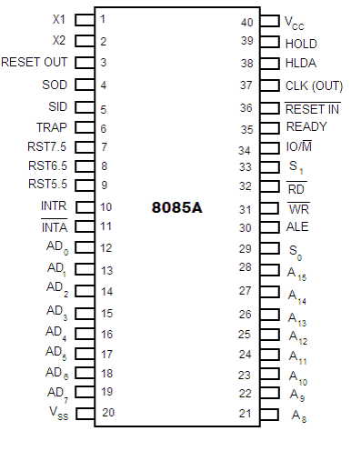
8085 Pin description
- Higher Order Address pins- A15 – A8
- The address bus has 8 signal lines A8 – A15 which are unidirectional.
- Lower Order Address/ Data Pins- AD7-AD0
- These are time multiplexed pins and are de-multiplexed using the pin ALE
- So, the bits AD0 – AD7 are bi-directional and serve as A0 – A7 and D0 – D7 at the same time.
- During the execution of the instruction, these lines carry the address bits during the early part, then during the late parts of the execution, they carry the 8 data bits.
- In order to separate the address from the data, we can use a latch to save the value before the function of the bits changes.
- Control Pins – RD, WR
- These are active low Read & Write pins
- Status Pins – ALE, IO/M (active low), S1, S0
- ALE (Address Latch Enable)-Used to de-multiplex AD7-AD0
- IO/M – Used to select I/O or Memory operation
- S1,S0 – Denote the status of data on data bus
- Interrupt Pins – TRAP, RST7.5, RST 6.5, RST 5.5, INTR, INTA
- These are hardware interrupts used to initiate an interrupt service routine stored at predefined locations of the system memory.
- Serial I/O pins – SID (Serial Input Data), SOD (Serial Output Data)
- These pins are used to interface 8085 with a serial device.
- Clock Pins- X1, X2, CLK(OUT)
- X1, X2– These are clock input pins. A crystal is connected between these pins such that fcrystal= 2f8085 where fcrystal= crystal frequency & f8085 = operating frequency of 8085
- CLK(OUT) – This is an auxiliary clock output source
- Reset Pins – Reset In (active low), Reset Out
- Reset In is used to reset 8085 whereas Reset Out can be used to reset other devices in the system
- DMA (Direct Memory Access) pins – HOLD, HLDA
- These pins are used when data transfer is to be performed directly between an external device and the main memory of the system.
- Power Supply Pins – +VCC, VSS
Leave a Reply